Kaixuan Vacuum Technology
Main Products: Manufacturing line for amorphous silicon PV solar cells, Sputtering coating line for Low-E or ITO glass, Manufacturing line for CIGS solar cell, Smart sputtering-optical coater of auto loading , Cathodic Arc PVD coater for hard film deposition, Sputtering web coater, Continuous production line for VIP sealing, Vacuum Sealing Machine for VIP, Wire-feeding web coater, Anti-fingerprint vacuum coater, Thermal evaporation coater, E-beam optical coater

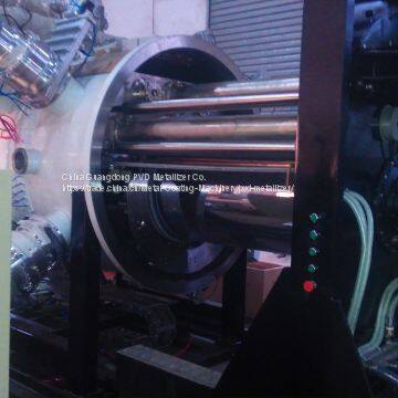
Sputter coating
Mr. Alex Li
May 31, 2017
Sputter coating
http://www.pvd-metallizer.com
Sputter coating in scanning electron microscopy is a sputter deposition process to cover a specimen with a thin layer of conducting material, typically a metal, such as a gold/palladium (Au/Pd) alloy. A conductive coating is needed to prevent charging of a specimen with an electron beam in conventional SEM mode (high vacuum, high voltage). While metal coatings are also useful for increasing signal to noise ratio (heavy metals are good secondary electron emitters), they are of inferior quality when X-ray spectroscopy is employed. For this reason when using X-ray spectroscopy a carbon coating is preferred.
Share
Recently Posted
-
Ion-assisted deposition
May 31, 2017Ion-assisted deposition http://www.pvd-metallizer.com In ion-assisted deposition (IAD), the substrate is exposed to a se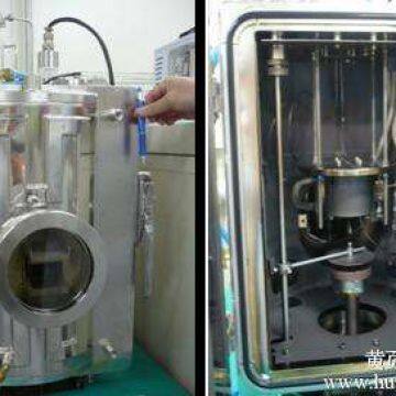 Read More
 -
Reactive sputtering
May 31, 2017Reactive sputtering http://www.pvd-metallizer.com In reactive sputtering, the sputtered particles undergo a chemical rea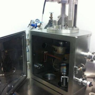 Read More
 -
Ion-beam sputtering
May 31, 2017Ion-beam sputtering http://www.pvd-metallizer.com Ion-beam sputtering (IBS) is a method in which the target is external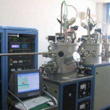 Read More
 -
Types of sputter deposition
May 31, 2017Types of sputter deposition http://www.pvd-metallizer.com Sputtering sources often employ magnetrons that util Read More

Contact Us
Recommended Products
-
 Complete Manufacturing Machines for Electro-chromic Smart Glass (Turn-Key Project)US$ 12000000 - 13000000MOQ: 1 Set
 -
Complete Manufacturing Line for CIGS Solar Cell (Turn-Key Project)NegotiableMOQ: 1 Piece
-
Roll-to-Roll Web Coating MachineNegotiableMOQ: 1 Piece
-
Vertical Continuous Sputtering LineNegotiableMOQ: 1 Piece
-
Experimental Evaporation Coater (with Resistance, E-beam, Induction and Ion Source, Etc.)NegotiableMOQ: 1 Piece


-
Experimental Magnetron Sputtering Coater With (DC/MF/RF/ion Source)NegotiableMOQ: 1 Piece
-
Pulsed Laser Deposition (PLD) MachineNegotiableMOQ: 1 Piece
-
Specialized Coating Equipment for EMI (Electro-Magnetic Interference) Film CoatingNegotiableMOQ: 1 Piece
-
Multi-functional MF Cathodic Arc PVD CoaterNegotiableMOQ: 1 Piece
-
Vacuum DryersNegotiableMOQ: 1 Piece


-
Paints and Varnishes for Vacuum Metalizing CoatingUS$ 9999 - 999999MOQ: 10 Tons
-
TS-2440CJXW Magnetron Sputtering Line for Aluminum Mirror CoatingUS$ 500000 - 600000MOQ: 1 Piece
-
Sputtering Line for AZO/ITO Glass CoatingUS$ 880000 - 9900000MOQ: 1 Piece
-
Sputtering Line for Touch Screen ProductionUS$ 880000 - 9900000MOQ: 1 Piece
-
Newly Invented Cathodic Arc PVD Coater for Razor Blade CoatingUS$ 88000 - 99000MOQ: 1 Piece


-
Vacuum Sealing Machine for VIPUS$ 110000 - 150000MOQ: 1 Piece
-
Production Line for VIP Vacuum Insulated PanelUS$ 1100000 - 1500000MOQ: 1 Piece
-
Magnetron Sputtering Web CoaterUS$ 990000 - 2100000MOQ: 1 Piece
-
Magnetron Sputtering CoaterUS$ 99000 - 210000MOQ: 1 Piece
-
Large-Scale Cathodic Arc PVD CoaterUS$ 770000 - 990000MOQ: 1 Piece